- 您现在的位置:买卖IC网 > Sheet目录224 > ESD9P5.0ST5G (ON Semiconductor)TVS UNIDIR 150MW 5.0V SOD-923
�� �
�
�ESD9P5.0ST5G�
�Transient� Voltage�
�Suppressors�
�ESD� Protection� Diodes� with� Ultra� ?� Low�
�Capacitance�
�The� ESD9P� Series� is� designed� to� protect� voltage� sensitive� components�
�that� require� low� capacitance� from� ESD� and� transient� voltage� events.�
�Excellent� clamping� capability,� low� capacitance,� low� leakage,� and� fast�
�response� time,� make� these� parts� ideal� for� ESD� protection� on� designs� that�
�utilize� high� ?� speed� lines� such� as� USB.�
�Specification� Features:�
�?� Low� Capacitance� 1.3� pF�
�?� Low� Clamping� Voltage�
�?� Small� Body� Outline� Dimensions:�
�0.039� ″� x� 0.024� ″� (1.00� mm� x� 0.60� mm)�
�?� Low� Body� Height:� 0.016� ″� (0.4� mm)�
�?� Stand� ?� off� Voltage:� 5� V�
�?� Low� Leakage�
�?� Response� Time� is� Typically� <� 1.0� ns�
�?� IEC61000� ?� 4� ?� 2� Level� 4� ESD� Protection�
�?� AEC� ?� Q101� Qualified� and� PPAP� Capable�
�?� This� is� a� Pb� ?� Free� Device�
�Mechanical� Characteristics:�
�CASE:� Void-free,� transfer-molded,� thermosetting� plastic�
�Epoxy� Meets� UL� 94� V� ?� 0�
�LEAD� FINISH:� 100%� Matte� Sn� (Tin)�
�MOUNTING� POSITION:� Any�
�QUALIFIED� MAX� REFLOW� TEMPERATURE:� 260� °� C�
�Device� Meets� MSL� 1� Requirements�
�http://onsemi.com�
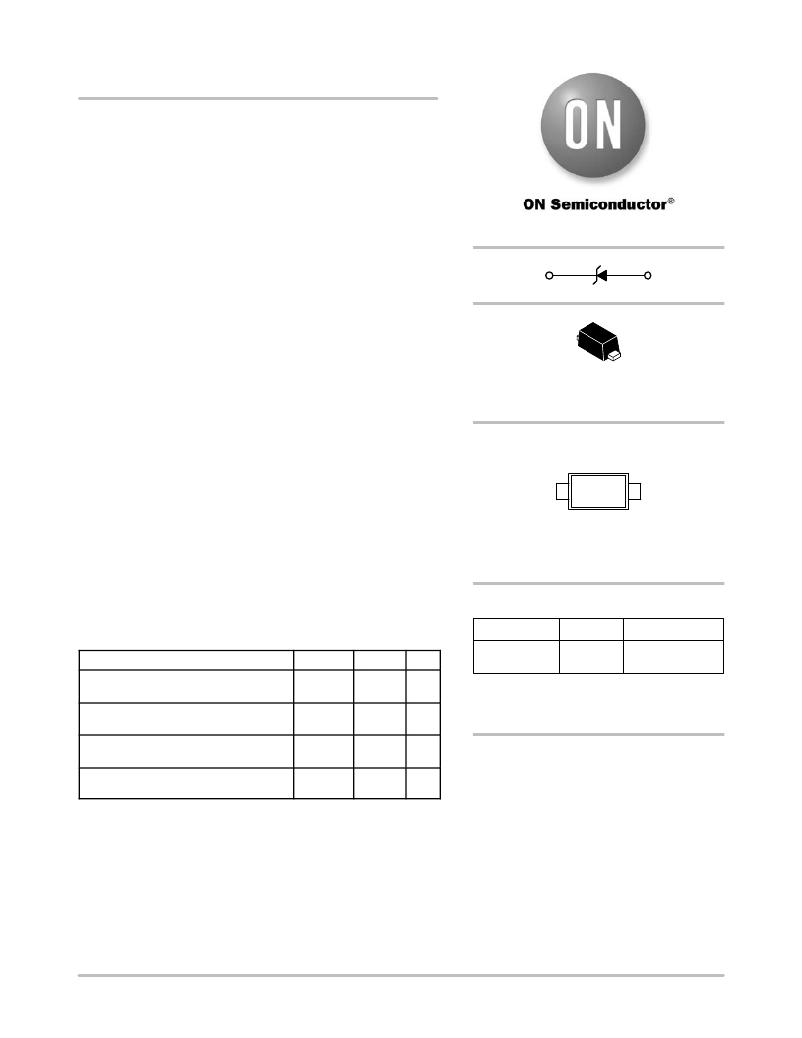
�SOD� ?� 923�
�CASE� 514AB�
�MARKING� DIAGRAM�
�TM�
�T� =� Specific� Device� Code�
�M� =� Date� Code�
�ORDERING� INFORMATION�
�MAXIMUM� RATINGS�
�Rating�
�Symbol�
�Value�
�Unit�
�Device�
�ESD9P5.0ST5G�
�Package�
�SOD� ?� 923�
�(Pb� ?� Free)�
�Shipping� ?�
�8000/Tape� &� Reel�
�IEC� 61000� ?� 4� ?� 2� (ESD)� Contact�
�Air�
�Total� Power� Dissipation� on� FR� ?� 5� Board�
�(Note� 1)� @� T� A� =� 25� °� C�
�Junction� and� Storage� Temperature� Range�
�Lead� Solder� Temperature� ?� Maximum�
�(10� Second� Duration)�
�°� P� D� °�
�T� J� ,� T� stg�
�T� L�
�±� 10�
�±� 15�
�150�
�?� 55� to�
�+150�
�260�
�kV�
�mW�
�°� C�
�°� C�
�?For� information� on� tape� and� reel� specifications,�
�including� part� orientation� and� tape� sizes,� please�
�refer� to� our� Tape� and� Reel� Packaging� Specifications�
�Brochure,� BRD8011/D.�
�DEVICE� MARKING� INFORMATION�
�See� specific� marking� information� in� the� device� marking�
�column� of� the� Electrical� Characteristics� tables� starting� on�
�page� 2� of� this� data� sheet.�
�Stresses� exceeding� Maximum� Ratings� may� damage� the� device.� Maximum�
�Ratings� are� stress� ratings� only.� Functional� operation� above� the� Recommended�
�Operating� Conditions� is� not� implied.� Extended� exposure� to� stresses� above� the�
�Recommended� Operating� Conditions� may� affect� device� reliability.�
�1.� FR� ?� 5� =� 1.0� x� 0.75� x� 0.62� in.�
�See� Application� Note� AND8308/D� for� further� description� of� survivability� specs.�
�?� Semiconductor� Components� Industries,� LLC,� 2013�
�January,� 2013� ?� Rev.� 1�
�1�
�Publication� Order� Number:�
�ESD9P5.0S/D�
�发布紧急采购,3分钟左右您将得到回复。
相关PDF资料
ESD9R3.3ST5G
TVS ESD ULT LOW CAP SOD-923
ESD9X7.0ST5G
TVS ESD ULT LOW CAP SOD-923
ESDR0502BT1G
IC LOW CAP ESD 2CH SC75
ESDR0502NMUTBG
TVS ARRAY LOW CAP 6UDFN
ESDR0524SMUTAG
IC ESD PROT LOW CAP 4CH 10UDFN
ESDR0544MDMR4G
4 CHAN LOW CAP ESD MICRO-10
ESM K12 1 5N C L130
SWITCH PUSH SPST-NO 0.1A 30V
EVN2000C
SWTCH TOP ROLLR PLUNGR SNAP SPDT
相关代理商/技术参数
ESD9R3.3ST5G
功能描述:TVS 二极管 - 瞬态电压抑制器 ESD PROT UNI SOD923 RoHS:否 制造商:Vishay Semiconductors 极性:Bidirectional 工作电压: 击穿电压:58.9 V 钳位电压:77.4 V 峰值浪涌电流:38.8 A 系列: 封装 / 箱体:DO-214AB 最小工作温度:- 55 C 最大工作温度:+ 150 C
ESD9R3.3ST5G
制造商:ON Semiconductor 功能描述:TVS-DIODE 150mW 7.8V SOD-923 制造商:ON Semiconductor 功能描述:TVS-DIODE, 150mW, 7.8V, SOD-923
ESD9X/BX.ST5G
制造商:ON 功能描述:ESD Protection Diode, SOD-923
ESD9X12ST5G
功能描述:TVS 二极管 - 瞬态电压抑制器 SOD-923 ESD PROT RoHS:否 制造商:Vishay Semiconductors 极性:Bidirectional 工作电压: 击穿电压:58.9 V 钳位电压:77.4 V 峰值浪涌电流:38.8 A 系列: 封装 / 箱体:DO-214AB 最小工作温度:- 55 C 最大工作温度:+ 150 C
ESD9X3.33ST5G
制造商:ON Semiconductor 功能描述:
ESD9X3.3ST5G
功能描述:TVS 二极管 - 瞬态电压抑制器 SOD-923 ESD PROT RoHS:否 制造商:Vishay Semiconductors 极性:Bidirectional 工作电压: 击穿电压:58.9 V 钳位电压:77.4 V 峰值浪涌电流:38.8 A 系列: 封装 / 箱体:DO-214AB 最小工作温度:- 55 C 最大工作温度:+ 150 C
ESD9X5.0ST5G
功能描述:TVS 二极管 - 瞬态电压抑制器 SOD-923 ESD PROT RoHS:否 制造商:Vishay Semiconductors 极性:Bidirectional 工作电压: 击穿电压:58.9 V 钳位电压:77.4 V 峰值浪涌电流:38.8 A 系列: 封装 / 箱体:DO-214AB 最小工作温度:- 55 C 最大工作温度:+ 150 C
ESD9X7.0ST5G
功能描述:TVS 二极管 - 瞬态电压抑制器 SOD-923 ESD PROTECTN RoHS:否 制造商:Vishay Semiconductors 极性:Bidirectional 工作电压: 击穿电压:58.9 V 钳位电压:77.4 V 峰值浪涌电流:38.8 A 系列: 封装 / 箱体:DO-214AB 最小工作温度:- 55 C 最大工作温度:+ 150 C